
Graphene, 2nm GAAFET Nodes, EUV Lithography & AFM • Engineering English
Praise sub-nanometer EUV critical dimension resolution, commend single-crystal CVD graphene transfers, and award the Certified Lead Nanotechnology Engineer Star!
Open Phase 1: Atomic Lexicon. Practice spoken pronunciation for the 6 nanotech decks (Quantum confinement, graphene & 2D materials, EUV lithography & 2nm GAAFET nodes, AFM microscopy, CVD/ALD synthesis, and cleanroom protocols).
Navigate to Phase 2: Fab Simulator. Execute 3 cleanroom workflows: 1. 2nm Gate-All-Around (GAAFET) EUV Lithography & High-NA Patterning, 2. Graphene & MoS2 CVD Growth, and 3. AFM Surface Topography & STS Spectroscopy.
Assign roles: Principal Scientist, EUV Scanner Operator, Metrology Specialist, and Cleanroom Protocol Lead in Phase 3: Fab Comms. Practice calling laser plasma alignments, Raman peak shifts, and safety oaths.
Debate Phase 4: Semiconductor Ethics (EUV export controls, PFAS wet bench chemical phase-out, rare earth recycling). Award the Phase 5: Certified Lead Nanotech Engineer Star!
| Engineer Matricula | Scientist Name | Role | Current Phase | Score | Stars | Cleanroom Status |
|---|---|---|---|---|---|---|
| Loading engineers in ISO Class 1 Fab... | ||||||
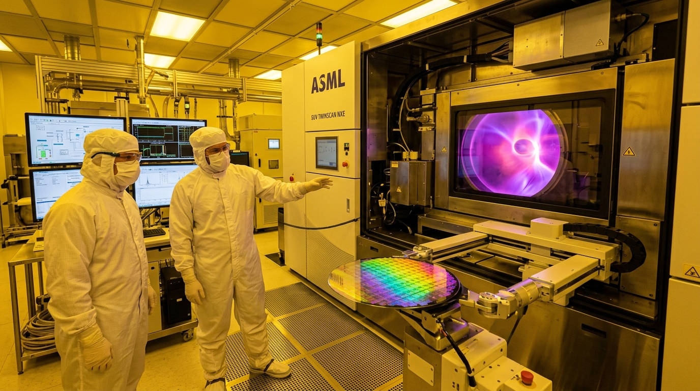
Step inside the cleanroom fab! Master atomic scale physics, 13.5nm Extreme Ultraviolet (EUV) photolithography, monolayer CVD graphene synthesis, and atomic force microscopy in fluent engineering English!
Click on the speaker icons to listen and practice English vocabulary for quantum confinement, graphene synthesis, EUV photolithography, and atomic force microscopy:
Tool: 0.55 High-NA EUV Scanner • Chemistry: Organotin Metal-Oxide Resist • Device: 2nm GAAFET Nanosheet Stack
Practice calling EUV laser plasma alignments, reporting Raman 2D band shifts, and taking the cleanroom engineering ethics pledge in professional English:
"Lithography Engineer: High-NA EUV scanner ready on wafer track #2. Tin droplet generator locked at 50 kilohertz; vacuum chamber pressure 10^-7 millibar."
Fab Director: "Laser pulse synchronization confirmed! Initiate 13.5 nanometer exposure sequence for the 2nm nanosheet layer!""Materials Scientist: Confocal Raman scan at 532 nanometers shows a sharp 2D peak at 2,680 cm^-1 with 2D to G intensity ratio exceeding 2.2."
Metrology Lead: "Outstanding! That confirms pristine single-crystal monolayer coverage with zero defect D-band signature!""Scientist A: I am an allotrope of carbon exactly one atom thick, with sp2 hybrid bonding, zero effective mass, and ballistic electron transport. What am I?"
Scientist B: "You are Graphene, the wonder 2D nanomaterial with massless Dirac fermions!""Defect Inspection Tech: Line-edge roughness on gate nanosheet #4 measured at 1.8 nanometers, exceeding our 1.2 nanometer threshold."
Process Engineer: "Adjust post-exposure bake temperature by two degrees and apply hydrogen radical surface smoothing!""All Engineers: We pledge to push the frontiers of atomic engineering with environmental responsibility, champion sustainable non-PFAS fabs, and safeguard technology for humanity!"
Principal Scientist: "Outstanding engineering leadership! You have officially earned your Certified Lead Nanotechnology Engineer Star Certificate!"Multilateral export regulations restrict advanced High-NA EUV lithography tool shipments, balancing national security against global academic research collaboration.
Fluorinated surfactants provide unmatched surface tension reduction in photoresist developers but persist indefinitely in groundwater ecosystems.
Fabricating High-k gate dielectrics requires Hafnium and Lanthanum, risking environmental degradation from destructive overseas open-pit mining.
High-aspect-ratio multi-walled carbon nanotubes present potential pulmonary toxicity risks if dry powders become airborne during synthesis.
🎉 CONGRATULATIONS! You have mastered atomic scale physics, 2nm High-NA EUV lithography, CVD graphene synthesis, and cleanroom engineering in professional English!